- Information
- AI Chat
Cadence schematic tutorials
Digital Integrated Circuits (ECE546)
North Carolina State University

Related Studylists
AICPreview text
ECE Department ECE 546 W. Rhett Davis
Analog Artist with HSPICE Tutorial
using the FreePDK
This tutorial will introduce you to the Cadence Environment: specifically Composer , Analog Artist and the Results Browser. It will also show you how to use the simulator HSPICE in stand-alone mode to make certain parts of your design exploration easier.
Proficient use of Cadence and Hspice will allow you to complete the projects and homework quickly and will make the class more fun. Practice is really the only way to achieve such proficiency. There are probably an infinite number of tricks and short-cuts to make the design process easier, or at least enough to fill a small book. No tricks or short-cuts are covered in this tutorial and it will be up to you learn more about the tool and how you can use it better for your needs.
Lastly, the screen-shots in this tutorial may vary slightly from what you will see. Refer to the text next to the screen-shot for up-to-date information. Note also that some screen-shots have been shrunk to make the page more readable. In this case, please click on the image to view its wiki-page, and click on the image again to download the full-size image.
Contents
- Create Aliases to Setup Your Environment .......................................................................................... 2
- Start the Cadence Design Framework ................................................................................................... 2
- Create the Schematics ........................................................................................................................... 3
- Create the myInverter schematic ................................................................................................... 5
- Place pmos instance ...................................................................................................................... 7
- Place nmos instance ...................................................................................................................... 7
- Place gnd and vdd instances .......................................................................................................... 8
- Place A and Z pins ........................................................................................................................ 8
- Place wires .................................................................................................................................... 9
- Create the myInverter symbol ....................................................................................................... 9
- Create the myInverterTestBench schematic ................................................................................ 10
- Place vdc instance ....................................................................................................................... 10
- Place vpulse instance .................................................................................................................. 11
- Place cap instance ....................................................................................................................... 12
- Place OUT pin ............................................................................................................................. 13
- Add Supply Nets, Wires, and a Label ......................................................................................... 13
- For more Information about Virtuoso ......................................................................................... 14
- Simulate the Schematic with HSPICE within Analog Artist .............................................................. 14
- Set up the Simulation Environment ............................................................................................ 14
- Choose a Simulator ..................................................................................................................... 15
- Copy the Design Variables ......................................................................................................... 15
- Setup the Transient Analysis ....................................................................................................... 16
- Complete the Online Tutorial ..................................................................................................... 16
ECE Department ECE 546 W. Rhett Davis
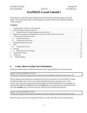
1. Create Aliases to Setup Your Environment
Before you start this tutorial, if you are a bash user, add the following line to the .bash_profile file in your home directory (note that these two lines should be joined on one line with a space between):
The line defines an alias that gives a command to setup your environment to use the FreePDK15 design- kit with the Cadence tools. You can set up other design-kits with other commands.
Before moving on, either source your .bash_profile f ile or log out and log back in.
2. Start the Cadence Design Framework
- Log in to a Linux machine. The setup for this tutorial is currently supported only on Linux machines.
- Create a directory to run this tutorial, called something like "adetut" (for Analog Design Environment Tutorial). Change to this directory.
- Type "add cadence2018 synopsys2018" at the command prompt. This will start a new command shell with the Virtuoso and HSPICE tools in the search path.
- Type "setup_freepdk15" at the command prompt. This will setup your directory by copying in various files that are needed to run the Cadence tools, including __ , lib , and cds. It will also define environment variables needed by the HSPICE libraries.
- Start the Cadence Design Framework by typing "virtuoso &" at the command prompt.
The first window that appears is called the CIW (Command Interpreter Window).
alias setup_freepdk15='source / afs/eos/lockers/research/ece/wdavis/tech/FreePDK15/cdslib/setup/setup'
$ mkdir adetut $ cd adetut $ add cadence2019 synopsys $ setup_freepdk $ virtuoso &
ECE Department ECE 546 W. Rhett Davis
the library will be created in the current directory. After you fill out the form, it should look something like this:
Click OK. Next, you will see a window asking you what technology you would like to attach to this library. Select "Attach to an existing technology library" and click OK. In the next window, select "NCSU_TechLib_FreePDK15".
You should see the library "ADETutorial" appear in the Library Manager.
ECE Department ECE 546 W. Rhett Davis
3. Create the myInverter schematic
Next, select the library you just created in the Library Manager and select File→New→Cell View.... We will create a schematic view of an inverter cell. Simply type in "myInverter" under cell-name and "schematic" under view. Click OK or hit "Enter". Note that the "Application" is automatically set to "Schematics L", the schematic editor.
Alternatively, you can select the "Schematics L" tool, instead of typing out the view name. This will automatically set the view name to "schematic".
ECE Department ECE 546 W. Rhett Davis
3. Place pmos instance
In the Add Instance window, select the pmos cell from the library NCSU_TechLib_FreePDK15. You may either type the values in or click Browse and find them in the Library Manager. After you select the cell, the "Add Instance" dialog will change to show the options for this cell. Note that most parameters are filled in automatically. The most important one for our purposes is "Number of Fins", which is set to 2 by default. The "Width" and "Length" fields are left blank, because they are not needed by the BSIM- CMG transistor model that we will be using. Place the PMOS cell in the Schematic Window.
3. Place nmos instance
Next, in the Add Instance window, select the nmos cell from the library NCSU_TechLib_FreePDK. Ensure that "Number of Fins" is set to 2. Place the cell in the Schematic Window.
ECE Department ECE 546 W. Rhett Davis
3. Place gnd and vdd instances
Next, from the analogLib library, place intances of gnd and vdd in the Schematic Window.
3. Place A and Z pins
- From the Schematic Window menu, select Create→Pin...
- In the Pin Names field , enter A Z
- In the Direction field, select input
- Click in the Schematic Window where you want the A pin to go. You will notice that the name A disappears from the Pin Names field after the pin is added.
- In the Direction field, select output
- Click in the Schematic Window where you want the Z pin to go.
ECE Department ECE 546 W. Rhett Davis
3. Create the myInverterTestBench schematic
Next, select the ADETutorial library again in the Library Manager and select File→New→Cell View... to create another Cellview called myInverterTestBench. Here’s what the test bench will look when complete. The instances that we will add are listed below the figure.
Description Library Cell View Device Under Test ADETutorial myInverter symbol Supply Nets analogLib vdd, gnd symbol Voltage_Sources analogLib vdc, vpulse symbol Passive Elements analogLib cap symbol
Start by placing an instance of myInverter. Then place the other elements. Be sure to pay special attention to the parameters specified in vdc , vpulse , and cap. These parameters are very important in simulation.
3. Place vdc instance
From the analogLib library, select vdc symbol. In the DC voltage field, enter VDD_VAL. By doing this, we define a variable that can be used later in simulation to determine the supply voltage. Note that the "V" will be inserted automatically. Place it in the Schematic Window.
ECE Department ECE 546 W. Rhett Davis
3. Place vpulse instance
Next, from the analogLib library, select vpulse symbol. Enter the following values in the form:
Voltage 1: 0 V Voltage 2: VDD_VAL V Delay Time: 0 s Rise Time: 10 p s Fall Time: 10 p s Pulse Width: 40 p s Period: 10 0p s
Place it in the Schematic Window.
ECE Department ECE 546 W. Rhett Davis
3. Place OUT pin
- From the Schematic Window menu, select Create→Pin...
- In the Pin Names field , enter OUT
- In the Direction field, select output
- Place it in the Schematic Window
3. Add Supply Nets, Wires, and a Label
- Add the vdd and gnd instances from analogLib as before, to match the myInverterTestBench schematic given in this tutorial. The schematic is given below again, for convenience.
- In the Schematic Window menu, select Create→Wire (narrow) and place wires to connect all instances.
- In the Schematic Window menu, select Create→Wire Name... and then, in the pop-up window, set the Names field to IN. Then click on the unnamed wire in the schematic to add the name. This defines a name for the net that can be used to reference simulation results. Note that if you
ECE Department ECE 546 W. Rhett Davis
wanted to define multiple labels, you could enter multiple names separated by spaces. Each time you click on a wire, it will add the next label in the list.
- Select File→Check and Save. Make sure to resolve any errors. Here again is how the final schematic should look.
3. For more Information about Virtuoso
If you would like to learn more about the schematic editor, you can read through the Virtuoso Schematic Editor User Guide that comes with the Cadence documentation. Start the documentation browser by typing
at the command prompt (note that the full path is currently required, because the command “cdnshelp” currently opens a browser with documentation for a different set of Cadence tools). Then click the icon
in the upper left corner to open the list of documents. Then select IC6→Virtuoso Schematic Editor→Virtuoso Schematic Editor User Guide in the browser window that appears. This should display the pages that you select.
If you find that you cannot view the figures correctly in the web browser, you can browse to the documentation directory in...
.. you will find PDF files for all of these documents. The cdnshelp documentation browser offers many more links for you to learn about the Cadence Design Framework.
4. Simulate the Schematic with HSPICE within Analog Artist
4. Set up the Simulation Environment
You are now prepared to simulate your circuit.
/afs/eos.ncsu/software/cadence2019/IC/tools/bin/cdnshelp &
/afs/eos.ncsu/software/cadence2019/IC/doc
ECE Department ECE 546 W. Rhett Davis
4. Setup the Transient Analysis
- From the ADE Window menu, select Analyses→Choose. You will see a “Choosing Analyses Pop-up window appear.
- Choose a transient (“tran”) analysis with start time 0, stop time 100 ps, and step 0 ps.
- Leave all other parameters as the default and click “OK”
4. Complete the Online Tutorial
At this point, I’ve run out of time in adapting this tutorial from the Web. Please visit eda.ncsu/wiki/FreePDK15:Analog_Artist_with_HSPICE and complete the tutorial, starting from the line that reads “Set your nodes to plot...” Where there are discrepancies, please refer to this document and follow the instructions here. For instance, note that the online tutorial uses the “hspiceD”, rather than “HSPICE”. We will use the “HSPICE” simulator. Note also that your circuit will run about 5 times slower than the one on the Wiki page.
Also, though not required, you may want to also look at the second tutorial, posted at eda.ncsu/wiki/FreePDK15:Schematic_Tutorial_2_-
ECE Department ECE 546 W. Rhett Davis
_ADE_L_Synopsys_HSPICE_integration, starting with the line that reads “You can do this by going to ADE L -> Results -> Plotting Assistant...”. The Plotting Assistant is another way to display outputs, which you may find more convenient. More importantly, the last part of this tutorial shows you how to use the HSPICE Measure Utility, which is very useful for completing homeworks #1 and #2.
Cadence schematic tutorials
Course: Digital Integrated Circuits (ECE546)
University: North Carolina State University


- Discover more from: